Cryo-FIB-SEM
A three-in-one imaging facility for opaque soft matter
The Cryogenic Focussed Ion Beam Scanning Electron Microscope (Cryo-FIB-SEM) is a multipurpose tool for imaging the micro- and nano-structure of complex fluids. A dedicated instrument scientist, Fraser Laidlaw, will work with you to prepare your sample and optimise the imaging protocol. On this page you can find out about the full range of capabilities of the instrument, see some example images, and get information on pricing.
About the instrument
We are delighted to introduce our Cryo-FIB-SEM facility, which is available to all researchers across the university, researchers from other academic institutions and external users including industry.
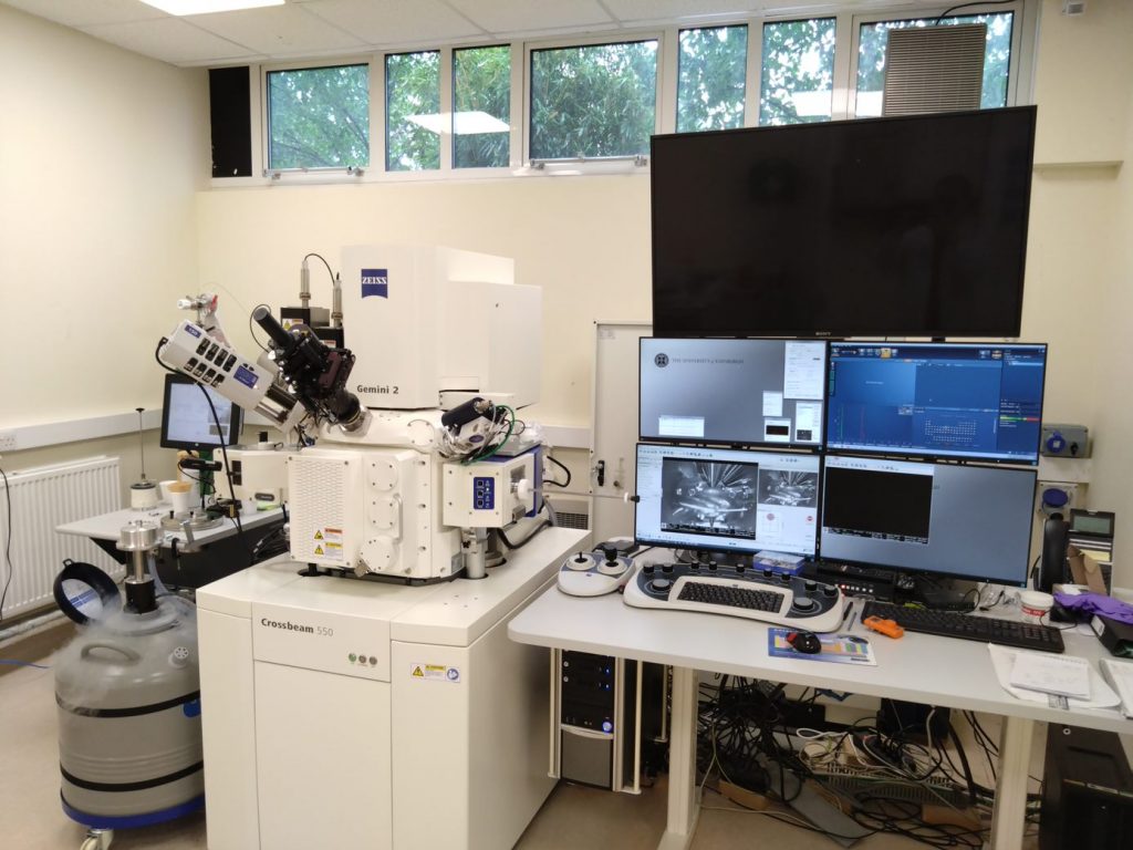
This Zeiss Crossbeam 550 FIB-SEM with cryogenic attachment from Quorum Technologies is one of only a few such instruments in the UK and offers a multitude of powerful techniques to extract as much information as possible from a large range of samples. The microscope offers resolution down to ~1nm, elemental contrast and identification, fast and accurate milling and patterning using the focussed ion beam (FIB), nanoscale tomography, TEM sample preparation and the ability to work on liquids, gels, polymers, biological matter and many other materials using the optional cryo mode.
The instrument was funded by EPSRC grant EP/P030564/1 in 2017.
Instrument Capabilities
The cryo-FIB-SEM is a versatile instrument and can work in a range of different modes along with a multitude of associated attachments, sample preparation techniques, and image post-processing. In the drop-down sections below you can find out more about these capabilities.
Imaging capabilites & attachments
- Zeiss’s Gemini electron optics and Field Emission Gun (FEG) source enables high resolution imaging capabilities even at low voltages and low/high currents – useful for beam sensitive and non-conductive samples (samples typically imaged under cryo conditions)
- Imaging at lower voltages typically leads to improved resolution and less signal from deeper in the sample (truer sample surface information). Lower accelerating voltage also lead to less charging of materials.
- Beam diameters of 0.9 nm at 15kV and 1.6nm at 1kV are possible using the FEG electron column.
- Microscope is equipped with 2 secondary electron detectors (InLens and SESI) and 2 backscatter detectors
- InLens – Secondary Electron (SE) detector within the electron column; high resolution SE imaging
- SESI (Secondary Electron Secondary Ion) – SE detector located at the side of the electron chamber
- ESB (Energy Selective Backscatter) detector – BSE detector located within the electron column – twin of the InLens detector. The energy of the backscatter electrons can be filtered remove low energy BSE electrons.
- BSD4 detector – Retractable BSE detector. Provides BSE imaging over a larger field of view than the ESB detector.
- The FIB column adds a 3rd spatial dimension to the imaging capabilities of the SEM transforming the microscope from a surface imaging technique to a volume imaging technique through the use of Automated serial slice sectioning techniques; FIB-SEM nano tomography.
- Ion source is Gallium, providing highly accurate and precise milling
- Produce 3D datasets of materials with z resolutions down to 3nm at room temperature and approximately 20 – 30nm under cryogenic conditions
Energy-dispersive X-ray (EDX) detector allows for the identification and mapping of elements within the sample
- Use “Point and ID” setting to take spectra from a point, or region, of the sample to identify and quantify the elemental composition in a localised region of the sample.
- Use “Linescan” settings to view how the composition of the samples changes along a direction/line of the sample surface.
- Use “Map” setting to map the spatial distribution of elements throughout a region of the sample
Enables TEM lamella sample preparation to be carried out (Hard materials only)
- Allows for ion induced deposition of platinum, carbon or silicon dioxide, or ion induced etching using water of XF2, within the microscope chamber
- Deposition of Pt and C layers are typically carried out prior to FIB milling to improve the quality of FIB milling by reducing charging and curtaining artefacts (vertical striations commonly observed in FIB cross sections).
- Ion beam induced etching increase the milling rates achieved in silicon materials (using the XF2 precursor gas) or carbon based materials (using the water precursor gas)
- Allows for the STEM imaging of TEM grids and very thin samples (typically < 100 nm thick)
- Load up to 12 TEM grids for STEM imaging; can be used to pre-screen samples prior to TEM
- Correlate SEM and FIB imaging with optical images of the sample
- Enhanced FIB-SEM nano tomography workflow of hard materials
- Automatic image stitching and data acquisition, allowing large areas of the sample to be imaged at high resolution
Sample preparation capabilities
- Samples can be plunge frozen into slush nitrogen with the Cryo preparation workstation
- Transfer frozen samples under vacuum into the on-column Cryo preparation chamber. This reduces frost/ice contamination on the sample from moisture content in the atmosphere
- Cryo preparation chamber attached to the side of the microscope, and allows for freeze fracture, sublimation and coating of samples in a single system
- Freeze samples in milliseconds; vitrifies samples, up to a few hundred um’s thick, allowing them to be imaged in as close to a native/natural state as possible
- Perform freeze substitution of biological samples
Image processing capabilities
- Reconstruct and visualise the 3D structure of materials from FIB-SEM nano tomography datasets
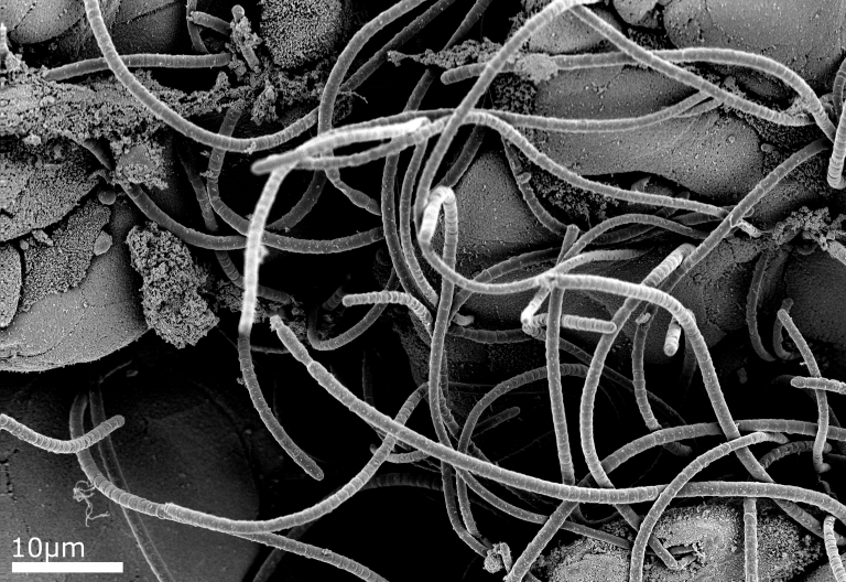
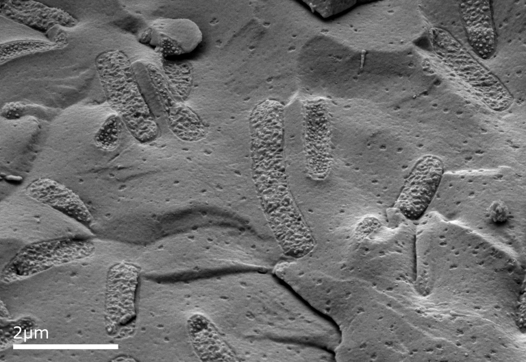
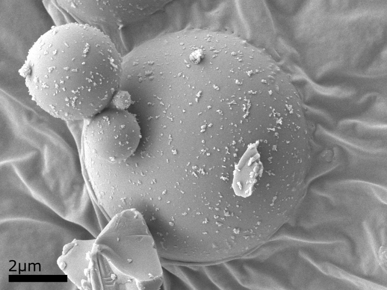
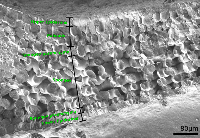
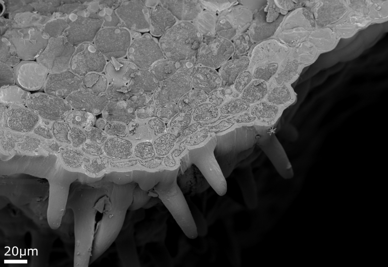
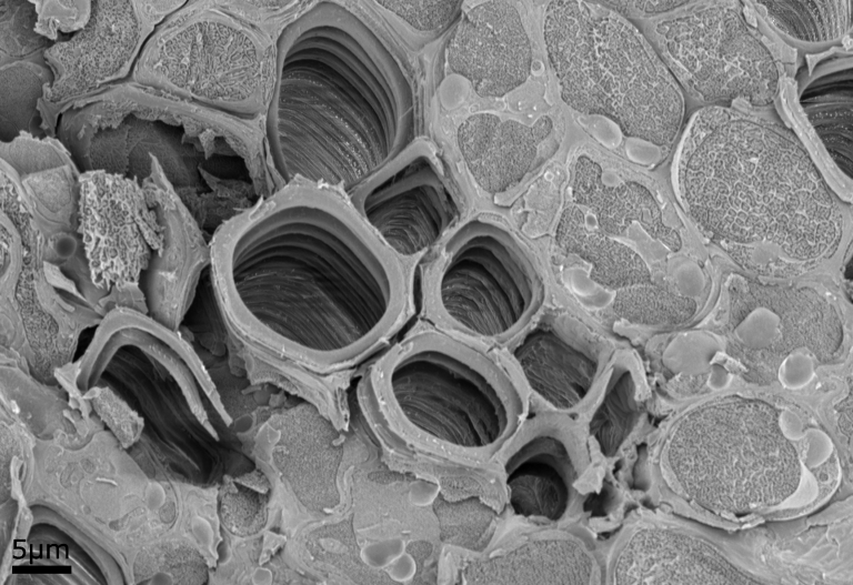
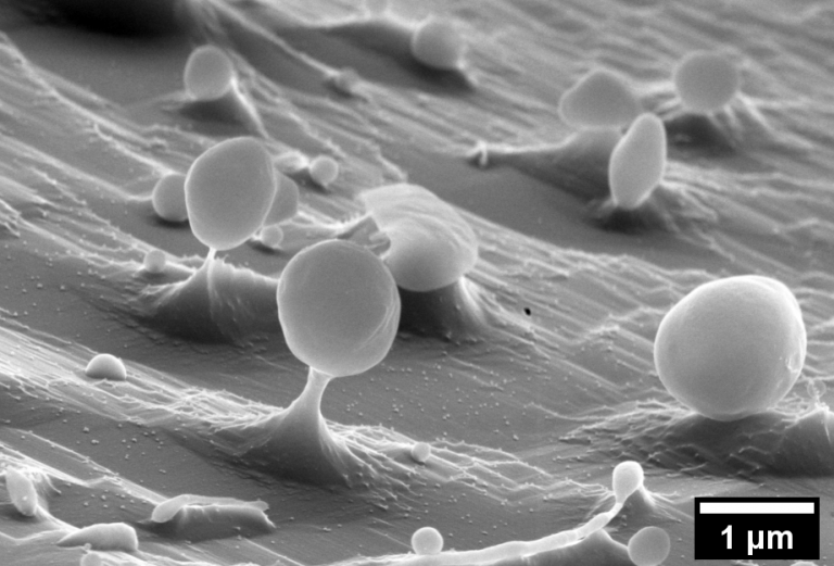
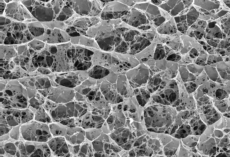
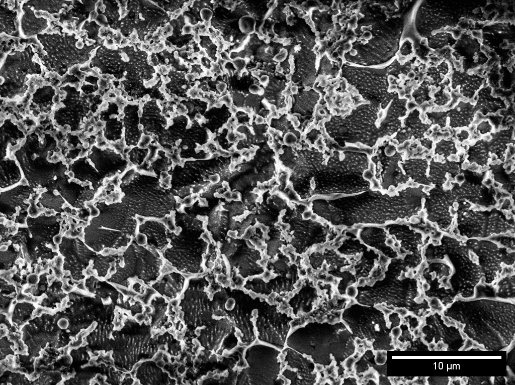
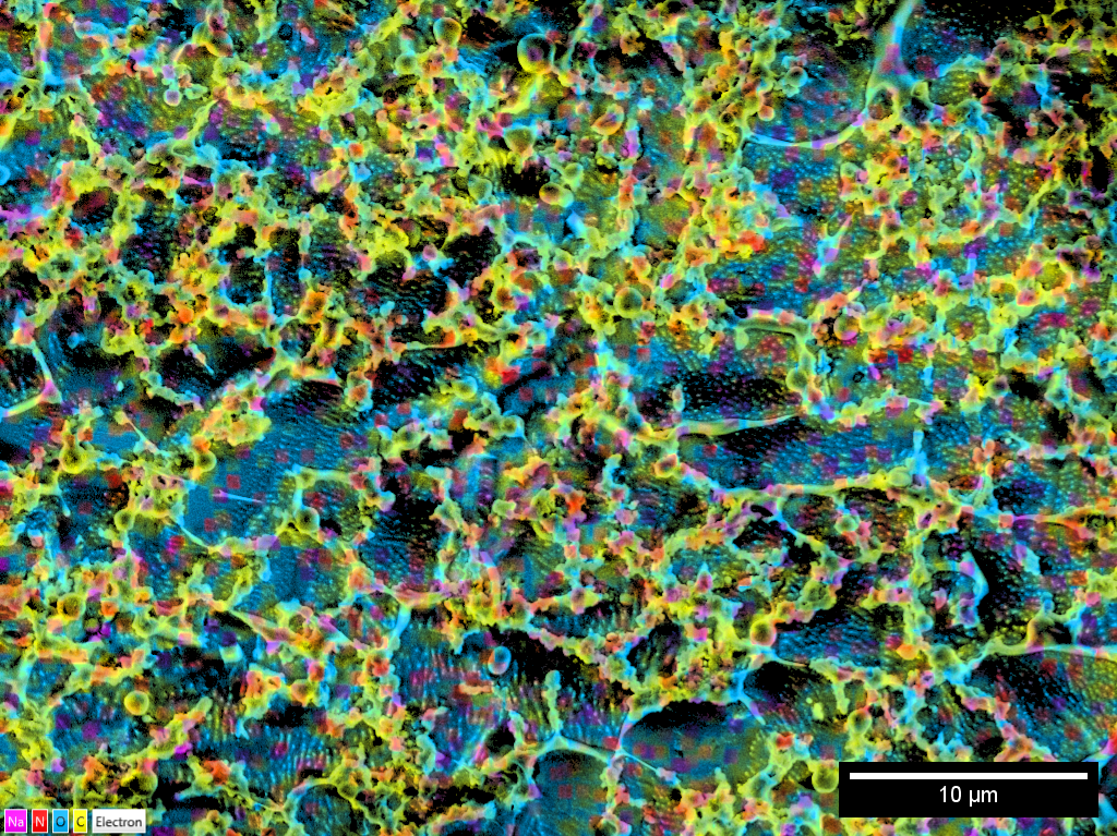
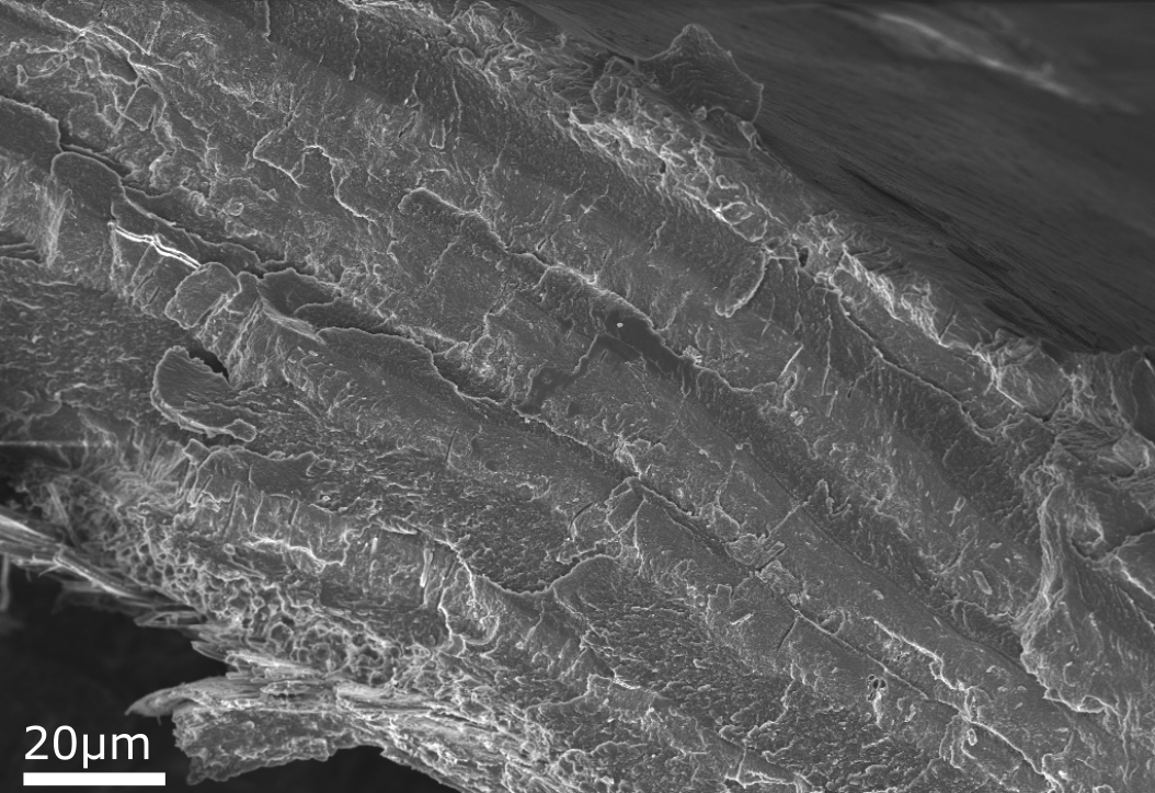
Example Images
Below are some example images from the cryo-FIB-SEM using a range of different samples, preparation and imaging techniques.
The Energy-dispersive X-ray (EDX) detector allows for the identification and mapping of elements within the sample. Use the slider below to compare a normal SEM image with the elemental mapping overlay, allowing the sample to be segmented in to carbon-rich areas (yellow) and oxygen-rich regions (blue). Sodium and nitrogen are also present in smaller quantities (pink and red respectively).
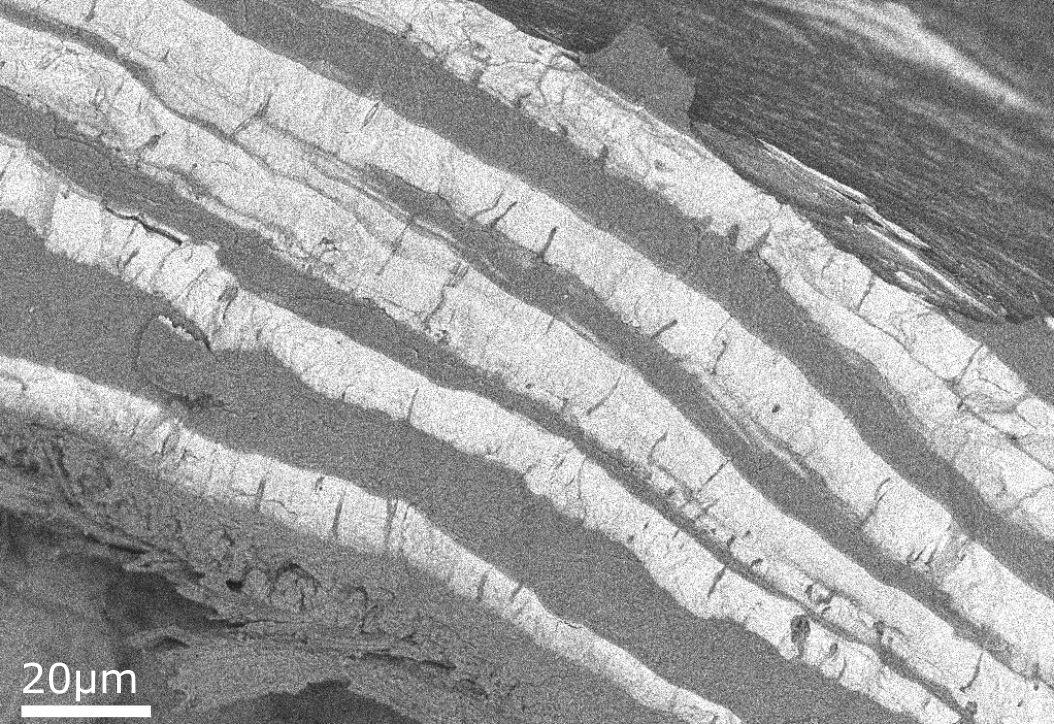
The image comparison below shows a cross section of a Brachiopod shell imaged using the InLens and Electron Backscattered (ESB) detectors.
Brachiopod shells are made up of alternating layers of organic and inorganic mineral layers. The InLens image shows the surface topography of the cross sectioned shell. It is just about possible to see the two layers in the InLens image however it isn’t possible to tell which layers are organic and which are mineral. The ESB image detects the backscattered electrons, and the contrast in that corresponds to atomic number; heavier atoms appear brighter in the image, as larger atoms have a larger backscatter coefficient, and light atoms appear dark, as they have a smaller backscatter coefficient. In the ESB image the bright bands are the mineral layers (mainly made up of calcium and phosphorus) while the darker bands are the organic layers (mainly carbon).
Multiple detectors can be used simultaneously to image a sample, such as the InLens and ESB detectors in this example, to detect both the Secondary electron (SE) and Backscatter electron (BSE) signal. This allows us to view both the surface topography and the elemental distribution of the same area of the sample. EDX imaging can then be used to determine what elements are present in the sample and their spatial distribution.
Pricing
We have techniques and equipment to characterise the physical properties of individual components so that we may understand how they interact and link this to the architecture of the microstructure observed in a product.
Please contact Dr Fraser Laidlaw (Fraser.Laidlaw@ed.ac.uk) for more information.
Please contact Dr Fraser Laidlaw (Fraser.Laidlaw@ed.ac.uk) for more information.
Please contact Dr Fraser Laidlaw (Fraser.Laidlaw@ed.ac.uk) for more information.
Additional Capabilities at ECFP
How can we help you?
Please get in contact with us to find out more about ECFP and whether we can help you.